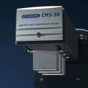

Description
Featrues and System specifications:
- Meas. technique: non-contact, junction photovoltage (JPV)
- Sample size: 100 to 156 mm (210mm option)
- Sample structure: np or pn junctions
- Measurement range: 10 Ω/sq. to 200 Ω/sq.
- Probe distance: 1.5 mm probe height above transport bel
- Wafer vertical position tolerance: < 400 μm
- Sample support: on belt
- Calibration: by wafers verified with four point probe
Options:
- Measurement module (incl. 1A-5A sheet resistance measurement heads)
- Industrial PC (Windows operation system) and peripherals
- CLS-1M emitter checker – option
- Wafer presence sensor (CMS only)
Wide variety of available interfaces to automation and MES:
- 24V optically isolated I/O, Ethernet interface
- Profibus
- OPC DA
- TCP/IP protocol, content can be XML or ASCII
- SQL database
- SECS/GEM