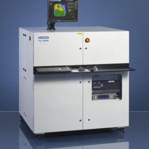

Description
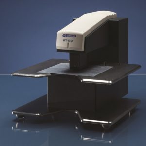
The WT-2000PVN can measure blocks and ingots, as well as wafers and cells. For measuring wafers and cells, people typically produce maps. When measuring blocks or ingots, people often produce only line scans, to save time, WT-2000PVN can do both.
Most producers of PV cells own a WT-2000PVN. It is extremely useful for:
- Engineering development and characterization
- Batch testing of production
- Comprehensive troubleshooting of production problems
Measurement techniques that can be integrated in WT-2000PVN:
- µ-PCD / carrier lifetime
- Measured parameter: carrier lifetime
- High resolution mapping and discrete point measurements
- Laser wavelength: 904nm
- SHR / sheet resistance
- Measured parameter: emitter sheet resistance
- Mapping and discrete point measurements
- LBIC / photovoltaic response, quantum efficiency, diffusion length
- High resolution mapping with 1 to 4 lasers
- Measured parameters:
Short circuit current
Direct and scattered reflectance
IQE and EQE
Diffusion length
- Eddy current resistivity
- Non-contact resistivity mapping
- Different resistivity range probes
- Bias light to µ-PCD