
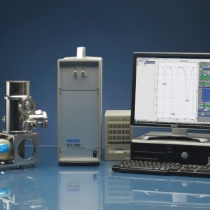
ACV-2200
(EN) The ACV systems provide 100% non-contact, non-destructive measurements for epi layer resistivity by patented technology. The physics behind the measurement is quite similar to C-V Schottky or Hg-probe, and thus the output is a traditional C-V doping profile. The difference is that the electrode does not touch the wafer, resulting in substantial cost savings of monitor wafers.
The model includes complete automation, powerful software and excellent measurement repeatability.
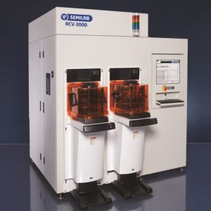
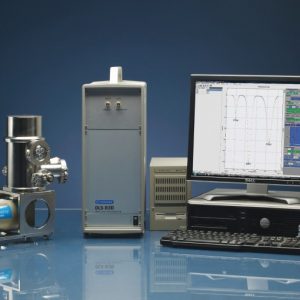
ACV-3000
(EN) The ACV systems provide 100% non-contact, non-destructive measurements for epi layer resistivity by patented technology. The physics behind the measurement is quite similar to C-V Schottky or Hg-probe, and thus the output is a traditional C-V doping profile. The difference is that the electrode does not touch the wafer, resulting in substantial cost savings of monitor wafers.
The model includes complete automation, powerful software and excellent measurement repeatability.

ACV-3100
(EN) The ACV systems provide 100% non-contact, non-destructive measurements for epi layer resistivity by patented technology. The physics behind the measurement is quite similar to C-V Schottky or Hg-probe, and thus the output is a traditional C-V doping profile. The difference is that the electrode does not touch the wafer, resulting in substantial cost savings of monitor wafers.
The model includes complete automation, powerful software and excellent measurement repeatability.


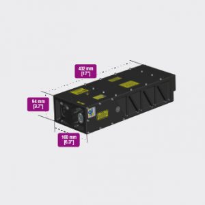
Centurion (40 mJ)
(EN) The Centurion is an air cooled, diode pumped laser, delivering 40 mJ energy in nanosecond pulses at repetition rates up to 100 Hz. Diode pumping reduces size, improves reliability, and eliminates most maintenance requirements.

Centurion (50 mJ)
(EN) The Centurion + is an air cooled, diode pumped laser, delivering 50 mJ energy in nanosecond pulses at repetition rates up to 100 Hz. Diode pumping eliminates the need of water, reduces size, improves reliability, and eliminates most maintenance requirements.
- Stable pulse energy in burst mode
- Variable attenuator and non-linear crystals integrated in laser head
- Homogeneous near field beam intensity profiles

CFR (200-400 mJ)
(EN) The CFR laser is a lamp pumped Nd:YAG laser featuring a degree of ruggedization not found in typical scientific lasers. The CFR design has been vibration tested and each laser is temperature cycled overnight, and tested again before shipping to ensure the laser arrives aligned and ready for use.
- 1064, 532, 355, 266, 213 nm and 1.57 µm available
- Alignment guaranteed
- Quick umbilical disconnects
- Compact and portable
- Gaussian or multimode resonators
- 50 million shots lamp lifetime guaranteed
- Built to withstand harsh environments
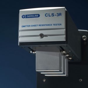
CLS
(EN) FAST NON-CONTACT MATERIAL CHARACTERIZATION AND PROCESS CONTROL
Emitter sheet resistance is a primary quality control parameter for silicon wafers in PV applications after emitter diffusion.
The CLS models, CLS-1A, CLS-3A, and CLS-5A, Emitter Sheet Resistance Testers allow measurement of sheet resistance at 1 to 5 points with the high throughput that meets the requirements of in-line quality control in fully automated cell production lines.
The CMS models, CMS-1A, CMS-3A, Emitter Sheet Resistance Testers allow measurement of wafers “on the fly”, i.e. conveyor belt does not stop during measurement. Therefore, they have the high throughput that meets the requirement of in-line quality control in fully automated cell production lines.
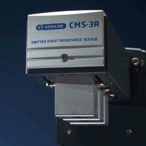
CMS
(EN) FAST NON-CONTACT MATERIAL CHARACTERIZATION AND PROCESS CONTROL
Emitter sheet resistance is a primary quality control parameter for silicon wafers in PV applications after emitter diffusion.
The CLS models, CLS-1A, CLS-3A, and CLS-5A, Emitter Sheet Resistance Testers allow measurement of sheet resistance at 1 to 5 points with the high throughput that meets the requirements of in-line quality control in fully automated cell production lines.
The CMS models, CMS-1A, CMS-3A, Emitter Sheet Resistance Testers allow measurement of wafers “on the fly”, i.e. conveyor belt does not stop during measurement. Therefore, they have the high throughput that meets the requirement of in-line quality control in fully automated cell production lines.

DBX-1000
Automatic Die Bonding System
The Kaijo DBX-1000 is an automated die bonder designed for the attachment of high-end epoxy dies with enhanced process features that enable highly efficient and cost-effective production.

DLS-1000
(EN) The DLS-1000 is an improved, high sensitivity system. It is eight times more sensitive than its predecessor, the DLS-83D.
The system offers a fully automatic measurement mode, as well as provides complete interpretation of the measured data, including impurity identification and concentration determination without any need for user interaction.
The Deep Level Transient Spectroscopy (DLTS) is the best technique for monitoring and characterizing deep levels caused by intentionally or unintentionally introduced impurities and defects in semiconductor materials and complete devices.
DLS-83D
(EN) The DLS-83D offers a fully automatic measurement mode, as well as provides complete interpretation of the measured data, including impurity identification and concentration determination without any need for user interaction.
The Deep Level Transient Spectroscopy (DLTS) is the best technique for monitoring and characterizing deep levels caused by intentionally or unintentionally introduced impurities and defects in semiconductor materials and complete devices. It is an extremely versatile method for determining all parameters associated with deep traps, including energy level, capturing cross-section and concentration distribution. It allows the identification of the impurities, and is capable of detecting contamination concentrations below 109 atoms/cm3.
DRL (100-700 mJ)
(EN) The DRL laser is a lamp pumped Nd:YAG laser based on
2 YAG rods pumped by 1 flash lamp each. This design enables a broad range of pulse energy and repetition rate combinations. Two versions of power supplies are used to cover the whole range of repetition rates. The DRL covers
20 – 200 Hz with pulse energies of 700 – 100 mJ at 1064 nm. The laser head is compact for easy integration and sealed to operate in various environments.
- 1064, 532 and 355 nm available
- Quick umbilical disconnects
- Compact
- Multimode resonators
- 100 million shots lamp lifetime guaranteed
- Sealed laser head to operate in various environments

DROPimage Advanced
(EN) DROPimage Advanced measures contact angle, surface energy, surface and interfacial tension, advancing and receding contact angle, surface dilatational elasticity and viscosity and is particularly well-suited for time-dependent and dynamic studies.

DROPimage CA
(EN) DROPimage CA is our entry-level software solution. This program ships standard with our Model 190 CA Goniometer and can be later upgraded to DROPimage Standard or Advanced if your requirements become more demanding. The two primary tools in DROPimage CA are the Contact Angle Tool and the Calibration Command as outlined below. Additional menus are available for: options, saving and opening images, data export, video setup, zooming, and baseline setup. DROPimage CA uses the same algorithms, video control, and methodology employed in the more advanced versions of DROPimage, but lacks the surface energy and surface tension tools.

DROPimage Standard
(EN)
DROPimage Standard ships with the Standard Goniometer (Model 200) and the Contact Angle Goniometer with Wafer Support (Model 400). It is also available as an upgrade for users of DROPimage CA. DROPimage Standard is well suited for contact angle and surface energy studies.
Below is a link to a playlist of videos that illustrates how easy it is to calibrate the instrument and take contact angle measurements using DROPimage Standard.

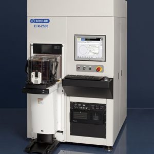
EIR-2500
(EN) The EIR-2500 is a unique automated epi thickness measurement tool with infared spectroscopic reflectometer for high throughput epi thickness measurement. Fully compliant to the relevant SEMI / CE standards. The EIR product line is based on smart, reliable electronics, which improves tool uptime and decreases maintenance needs.